EE220 2024 Noise Analysis and Simulation: Difference between revisions
No edit summary |
|||
| Line 8: | Line 8: | ||
* What is the transistor's <math>g_m</math> and <math>V^*=\frac{2I_D}{g_m}</math>? | * What is the transistor's <math>g_m</math> and <math>V^*=\frac{2I_D}{g_m}</math>? | ||
Run a noise analysis from <math>1\mathrm{Hz}</math> to <math> | Run a noise analysis from <math>1\mathrm{Hz}</math> to <math>1\mathrm{THz}</math>. | ||
* Plot the drain current noise power spectral density, <math>\frac{\overline{i_{dn}^2\left(f\right)}}{\Delta f}</math>. | * Plot the drain current noise power spectral density, <math>\frac{\overline{i_{dn}^2\left(f\right)}}{\Delta f}</math>. | ||
** Identify the regions where thermal noise and flicker noise dominates. | ** Identify the regions where thermal noise and flicker noise dominates. | ||
Latest revision as of 06:52, 9 October 2024
- Instructions: This activity is structured as a tutorial with an activity at the end. Should you have any questions, clarifications, or issues, please contact your instructor as soon as possible.
- At the end of this activity, the student should be able to:
- Perform noise simulations using Cadence Spectre using the GlobalFoundries 22nm FDSOI design kit.
Activity 1: NMOS Noise
Bias a 0.8V SLVT NMOS transistor with and . For a width of and a length of :
- What is the resulting DC drain current?
- What is the transistor's and ?
Run a noise analysis from to .
- Plot the drain current noise power spectral density, .
- Identify the regions where thermal noise and flicker noise dominates.
- What is the flicker noise corner?
- Estimate the value of .
- Estimate the value of
- What is the total integrated drain current noise power?
Recall that the MOSFET drain current noise can be modeled as:
Change the length of the transistor to and . Identify and explain any changes in the drain current noise power spectral density.
- Repeat for the LVT and regular-VT NMOS transistors. Did you notice any differences in noise behavior?
Activity 2: PMOS Noise
Repeat Activity 1 but with 0.8V PMOS transistors with the same sizes, and with and .
Activity 3: Cascode Amplifier Noise Analysis
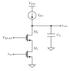
Consider the cascoded NMOS amplifier (biased with an ideal current source) shown in Fig. 1. Ignoring all other capacitances except , and given the small-signal parameters , , and :
- Calculate the small-signal gain of the cascode amplifier, . Assume and .
- Calculate the noise spectral density, , and the total integrated output noise, . Assuming that and , and that the flicker noise is zero.
- Repeat (2) but with finite and . How does this affect the output noise?
Activity 4: Input-Referred Noise
Given the gate-source capacitance, , of transistor of the cascode amplifier in Fig. 1, calculate:
- The input equivalent voltage noise generator, .
- The input equivalent current noise generator, .
Note that when calculating the output noise, you can assume that and , but when calculating the gains, assume finite and .
Report Guide
Write up a report (maximum of 5 pages including figures) answering the questions above. Include annotated graphs if needed.


