Activity: MOS Transistor Characteristics: Difference between revisions
| (2 intermediate revisions by the same user not shown) | |||
| Line 23: | Line 23: | ||
These figures were generated from the simulation output using this [https://github.com/louisalarcon/ee220/blob/0e8e49deb82c8e9e38308c7e1a127c7cfc8320fb/cidr/activity-4-mos-characteristics.py Python script]. Please feel free to edit and adopt to your needs. | These figures were generated from the simulation output using this [https://github.com/louisalarcon/ee220/blob/0e8e49deb82c8e9e38308c7e1a127c7cfc8320fb/cidr/activity-4-mos-characteristics.py Python script]. Please feel free to edit and adopt to your needs. | ||
Comment on the effect of process variations and changing <math>V_{DS}</math> on the transfer characteristics, specifically the value of the drain current, and the operating regions, when: | Comment on the effect of process variations and changing <math>V_{DS}</math> on the transfer characteristics, specifically the value of the drain current, and the operating regions, when you: | ||
* Change <math>V_{DS}</math> to 0.45V and 1.35V | * Change <math>V_{DS}</math> to 0.45V and 1.35V | ||
* Change <math>nf</math> from 1 to 10 | * Change <math>nf</math> from 1 to 10 | ||
Do the simulation results agree with what you expect? Why? | |||
== Activity 2: NMOS Output Characteristics == | == Activity 2: NMOS Output Characteristics == | ||
| Line 40: | Line 40: | ||
== Activity 4: PMOS Transfer and Output Characteristics == | == Activity 4: PMOS Transfer and Output Characteristics == | ||
Create a schematic to generate the transfer and output characteristics of a 1.8V LVT PMOS transistor with width <math>W=10\mathrm{\mu m}</math>, length <math>L=0. | Create a schematic to generate the transfer and output characteristics of a 1.8V LVT PMOS transistor with width <math>W=10\mathrm{\mu m}</math>, length <math>L=0.35\mathrm{\mu m}</math>, and number of fingers <math>nf=1</math>. Then repeat activities 1, 2, and 3 (with <math>L=0.70\mathrm{\mu m}</math> and <math>L=1.05\mathrm{\mu m}</math>). | ||
== Report Guide == | == Report Guide == | ||
Latest revision as of 00:18, 3 October 2022
Activity: MOSFET Characteristic Curves
- Instructions: This activity is structured as a tutorial with an activity at the end. Should you have any questions, clarifications, or issues, please contact your instructor as soon as possible.
- At the end of this activity, the student should be able to:
- Generate the characteristic curves of NMOS and PMOS transistors.
MOS Transfer Characteristics
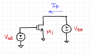
The transfer characteristics of an NMOS transistor is the relationship between the gate-source voltage, which serves as the "input" port of a common-source amplifier, and the "output" drain current. To get you started, here is an xschem schematic to simulate the transfer characteristic of our sky130 low-threshold voltage (LVT) NMOS transistor. The NMOS transistor in the sample schematic has the following parameters: a width , a length , and the number of fingers .
Activity 1: MOS Operating Regions
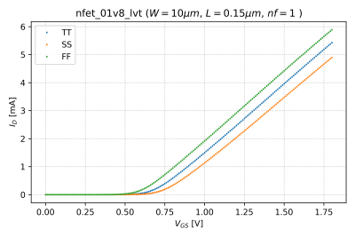
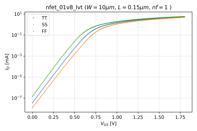
By modifying the sample schematic, plot out the NMOS transfer characteristics for the TT, FF, and SS corners, as shown in Figs. 2 and 3. Graphically, identify the following regions:
- The quadratic or square-law region
- The velocity saturation region
- The subthreshold or weak inversion region
- The moderate inversion region.
These figures were generated from the simulation output using this Python script. Please feel free to edit and adopt to your needs.
Comment on the effect of process variations and changing on the transfer characteristics, specifically the value of the drain current, and the operating regions, when you:
- Change to 0.45V and 1.35V
- Change from 1 to 10
Do the simulation results agree with what you expect? Why?
Activity 2: NMOS Output Characteristics
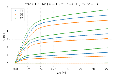
The given SPICE file and Python script also plots the NMOS output characteristics, shown in Fig. 4. Modify the sample schematic and plot the NMOS TT, FF, and SS corner output characteristics and graphically, identify the saturation region, the subthreshold region, and the linear or resistive region. Comment on the effect of process variations.
Activity 3: Increasing Channel Length
What happens when you increase the transistor length to and ? Plot out the resulting transfer and output characteristics, and comment on the resulting drain currents, the operating regions, and the effect of process variations.
Activity 4: PMOS Transfer and Output Characteristics
Create a schematic to generate the transfer and output characteristics of a 1.8V LVT PMOS transistor with width , length , and number of fingers . Then repeat activities 1, 2, and 3 (with and ).
Report Guide
Write up a report (maximum of 5 pages including figures) answering the questions above. Include annotated graphs showing the different regions of operation for both the NMOS and PMOS transistors.
Submission
This activity is for both graduate and undergraduate students. For UP students, the submission bin link will be posted in Piazza.


