Design: A Simple Common-Source Amplifier
Revision as of 15:37, 12 October 2022 by Louis Alarcon (talk | contribs) (→Activity 1: Transistor Intrinsic Gain)
- Instructions: This activity is structured as a tutorial with an activity at the end. Should you have any questions, clarifications, or issues, please contact your instructor as soon as possible.
- At the end of this activity, the student should be able to:
- Design a simple common-source amplifier.
Activity 1: Transistor Intrinsic Gain
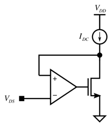
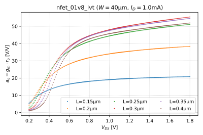
For a certain DC drain current, , and DC drain-to-source voltage, , we can determine the intrinsic NMOS small-signal gain, .
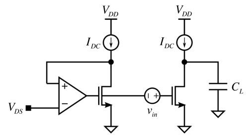
Design: A Common-Source Amplifier
Report Guide
Write up a report (maximum of 5 pages including figures) answering the questions above. Include annotated graphs if needed.
Submission
This activity is for both graduate and undergraduate students. For UP students, the submission bin link will be posted in Piazza.


