Design: A Simple Common-Source Amplifier
- Instructions: This activity is structured as a tutorial with an activity at the end. Should you have any questions, clarifications, or issues, please contact your instructor as soon as possible.
- At the end of this activity, the student should be able to:
- Design a simple common-source amplifier.
Activity 1: Transistor Intrinsic Gain
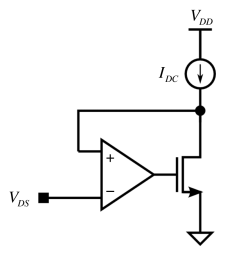
We can determine the intrinsic NMOS small-signal gain, , for a desired DC operating point, i.e for a given drain current, , and drain-to-source voltage, . This implies a certain gate-to-source voltage, . For square-law devices, we can easily calculate the required that corresponds to and . However, for deep submicron devices that do not follow the square law, we can either run simulations to determine this , or instead, we can let SPICE calculate for us. As seen in Fig. 1, we can use negative feedback to obtain the appropriate .
Tasks: (Use , , and )
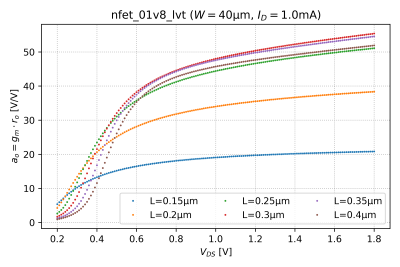
- Using NGSPICE, sweep from 200mV to 1.8V, and plot as a function of .
- From the vs. plot, derive the NMOS instrinsic gain, , as a function of .
- Repeat for transistor lengths of , , , , and , and generate the graphs in Fig. 2.
Design: A Common-Source Amplifier
Report Guide
Write up a report (maximum of 5 pages including figures) answering the questions above. Include annotated graphs if needed.
Submission
This activity is for both graduate and undergraduate students. For UP students, the submission bin link will be posted in Piazza.


