Activity: Noise Analysis
Revision as of 09:53, 6 November 2022 by Louis Alarcon (talk | contribs) (→Activity 3: Noise Analysis)
- Instructions: This activity is structured as a tutorial with an activity at the end. Should you have any questions, clarifications, or issues, please contact your instructor as soon as possible.
- At the end of this activity, the student should be able to:
- Perform noise simulations using NGSPICE.
Activity 1: NMOS Noise
Bias a 1.8V LVT NMOS transistor with and . For a width of and a length of :
- What is the resulting DC drain current?
- What is the transistor's and ?
Run a noise analysis from to . You can use this sample schematic as a starting point.
- Plot the drain current noise power spectral density.
- Identify the regions where thermal noise and flicker noise dominates.
- What is the flicker noise corner?
- Estimate the value of .
- Estimate the value of
- What is the total integrated drain current noise power?
Recall that the MOSFET drain current noise can be modeled as:
Change the length of the transistor to . Identify and explain any changes in the drain current noise power spectral density.
Activity 2: PMOS Noise
Repeat Activity 1 but with a 1.8V LVT PMOS transistor with the same size and with and .
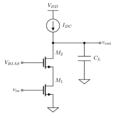
Activity 3: Cascode Amplifier Noise Analysis
Activity 4: Input-Referred Noise
Report Guide
Write up a report (maximum of 5 pages including figures) answering the questions above. Include annotated graphs if needed.
Submission
This activity is for both graduate and undergraduate students. For UP students, the submission bin link will be posted in Piazza.


