Activity: MOS Design Parameters
- Instructions: This activity is structured as a tutorial with an activity at the end. Should you have any questions, clarifications, or issues, please contact your instructor as soon as possible.
- At the end of this activity, the student should be able to:
- Obtain the small signal design parameters of NMOS and PMOS transistors.
Activity 1: Small Signal Models
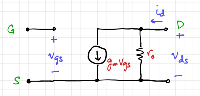
Most of the time, we are interested in the small signal behavior of our amplifiers, i.e. what happens to the amplifier voltages and currents as we introduce small disturbances (information carrying signals) at the input. To gain intuition and to facilitate circuit analysis using nonlinear devices, we linearize our circuits to obtain the two-port model shown in Fig. 1. For MOSFETs at low frequencies, the two-port model is composed of the transconductance, and the output resistance.
Transconductance
Transconductance is defined as:
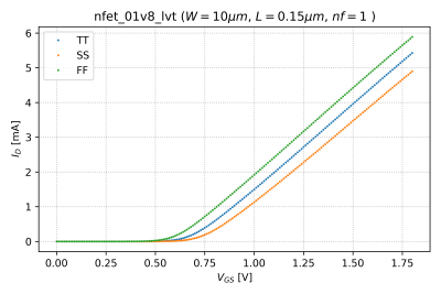
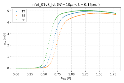
This is the slope of the transfer characteristic curves. Thus, by numerically differentiating the vs. curve shown in Fig. 2 for an NMOS transistor with a width , a length , and with , we can obtain the transconductance plot shown in Fig. 3.
Output Resistance
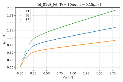
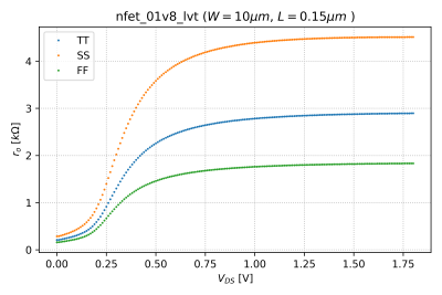
Similarly, we can take the derivative of the output characteristics, shown in Fig. 4 for , to get the output resistance, which is defined as:
The output resistance as a function of is shown in Fig. 5 for .
Answer the following questions:
- Given the transconductance plot in Fig. 3, why is there a peak in the transconductance curve? What is causing this?
- Generate Fig. 3, but on a logarithmic y-axis. Is this what you expect for ? Explain.
- Plot for and . Does the transconductance change with ? Is this the behavior you expect? Explain.
- Plot the output resistance for and . Do you see any changes in the the effects of process variations? What do you think is causing this behavior?
Activity 2: Power Efficiency
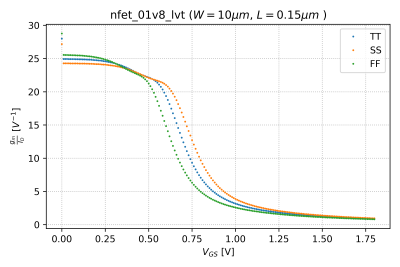
We can define a power efficiency figure of merit (FoM) for our transistors that quantifies the DC current cost, i.e. , of achieving a certain transconductance, . Mathematically, we can express this as , and is plotted vs. , as shown in Fig. 6.
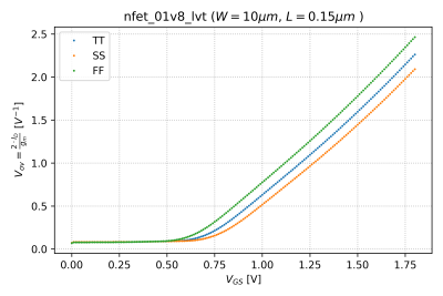
An alternative form of this power efficiency metric, is . This alternative FoM is plotted against , as shown in Fig. 7.
Answer the following questions:
- Why does the plot , shown in Fig. 6, flatten out at low ?
- Recreate Fig. 6 but with and . Does the maximum value of change? Is this what you expect? Why or why not?
Activity 3: Aggregate Figure of Merit
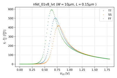
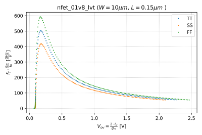
Increasing the power efficiency of the transistor moves it further into its subthreshold region, leading to lower transition frequencies. Thus, in choosing the value of , we can define an aggregate figure of merit that takes into account both the power efficiency and transition frequency, as . This figure of merit is plotted against , as shown in Fig. 8.
Notice that the peak occurs at different values over corners. However, if we plot it against as seen in Fig. 9, we get a consistent peak, at around .
Answer the following questions:
- It seems that the peak occurs in the moderate inversion region. Plot this figure of merit for and . Does the peak still appear in the moderate inversion region? Is this what you expected? Why?
- For and , does the peak occur at the same over the FF, TT, and SS corners? Is this what you expected? Why?
Activity 4: PMOS Small Signal Parameters
Repeat Activities 1, 2, and 3 for a 1.8V LVT PMOS transistor with a width , a length , and with . When varying PMOS length, use and .
Report Guide
Write up a report (maximum of 5 pages including figures) answering the questions above. Include annotated graphs if needed.
Submission
This activity is for both graduate and undergraduate students. For UP students, the submission bin link will be posted in Piazza.
