RISC-V processor for machine learning
Incorporating machine learning capabilities in wireless sensor networks (WSNs) will require an increase of computational capabilities of the sensor nodes. However, most WSNs use commercial, off-the-shelf Microcontroller Units (MCUs) that are low cost and have low power consumption but have limited processing capabilities[1] or System on Chips (SoCs) with high performance and low power consumption but has fixed configuration.[2] Due to these constraints, FPGA-based processors are currently being considered due to its rapid prototyping, dynamic reconfiguration, and acceleration of processing. It should be noted, though, that FPGA-based designs have greater power consumption as compared to SoC and MCU implementations. However, recent research shows that increasing computational capabilities at the network edge can shorten packet lengths, reduce sent packets[3], and reduce network usage, thus, significantly lowering the overall energy consumption of the sensor node.[4]
To provide flexibility in the design of the processor, the RISC-V Instruction Set Architecture (ISA)[5], an open-source, royalty-free ISA, offers a simple, modular and stable architecture that is ideal for a wide variety of embedded and IoT applications. RISC-V implementation is composed of a mandatory base ISA called RV32I and a number of ISA extensions that can be added depending on the application that it will be used for. For machine learning applications, RISC-V has a vector extension suitable for parallel computations.
For this project, an FPGA-based RISC-V processor with vector extension will be implemented.
Baseline Processor Design
The design of the baseline processor is based on the paper of M.J. Neri, et al[6] from EEEI in the University of the Philippines, Diliman. It is an FPGA-based RISC-V processor with integer multiplication and division extension and compressed instruction extension, thus, an RV32IMC processor. The processor is pipelined with 5 stages as shown in Figure 2.
The Instruction Fetch or IF stage contains the Instruction Memory and the Program Counter (PC) blocks. The Instruction Memory block was halfword-addressable so the PC can be incremented by 2 or by 4 whether instructions are compressed or not. It also has Interrupt handling capabilities. This is done by saving the current PC address to the Save PC Register whenever an interrupt is detected.
The Instruction Decode or ID stage includes the Decode and Control Logic block, a Register File (RF) block with 31 general-purpose registers, and a Shift, Sign Extension, and Shuffle block. A Branch Prediction block which uses the concept of bimodal branch prediction and Branch History Table (BHT) is also available.[7] This block also handles control hazards.
In the Execution or EXE stage, all operations, including branch comparison, are handled by the Arithmetic Logic Unit (ALU) and a Divider block with 38-46 cycle latency. It also includes a Store block which formats the data that will be stored in the Data Memory.
The MEM stage contains the Data Memory and the Load block, which formats the obtained data depending on the load instruction used.
Lastly, the Write Back or WB stage uses a single multiplexer to select the data that will be written to the Register File. A Forwarding Unit is also included to solve possible data dependencies between instructions.
The list of instructions that were implemented in this processor, the RV32I base integer, the “M” standard extension and the “C” standard extension instruction sets, are found in The RISC-V Instruction Set Manual.[8]
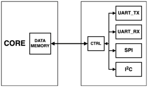
The RV32IMC processor is also designed with the following communication blocks: an Inter-integrated Circuit (I2C), a Serial Peripheral Interface (SPI), and a Universal Asynchronous Receiver/Transmitter (UART). The protocol controller of these blocks are interfaced to the processor through memory mapping as shown in Figure 3.
RISC-V Vector Coprocessor
The initial RISC-V vector coprocessor design implements a limited integer-only subset of the RISC-V Vector Extension. It supports 128 bit wide vector registers and is configured by default to process 128 bits per cycle for arithmetic instructions and up to 128 bits per cycle for memory read/write operations. With the implementation of forwarding for dependent elements, it is expected to have a speedup of up to 16x working on 8-bit integer workloads, and up to 4x on 32-bit workloads, compared to the baseline processor.
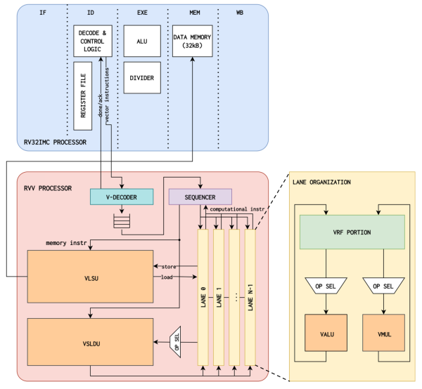
The coprocessor is intended to be integrated into a modified baseline RV32IMC processor as shown in Figure 4. The baseline processor detects vector instructions, and then sends those to the coprocessor for decoding and execution. The coprocessor is then responsible for sending and receiving data with the baseline processor and its internal data memory module, which facilitates transfers of data to and from memory, and between scalar and vector register registers.
The vector coprocessor is divided into distinct blocks, with respective functionalities, that work together to execute every instruction that is fed into it. Once an instruction is issued to the vector coprocessor, it is fed into the internal decoder, V-Decoder. It generates control signals and decodes the instruction, such as its type, source and destination registers, and the specific operation to be performed.
The decoded instruction is then passed to the sequencer, which is responsible for dispatching instructions to the corresponding functional unit. Should there be a data hazard, or an unavailable corresponding functional unit, it is placed into the instruction queue until the conflict is resolved.
The functional units perform operations on inputs, which can be read from vector register groups. Scalar registers or immediate values encoded as part of the instruction can also be used as inputs. Once these are complete, the resulting outputs can then be written back into the output vector register group.
Each vector register stores individual elements together in packed data. These can be grouped together in register groups of up to 8 registers, resulting in an effective vector length of up to 1024 bits, based on a vector register width of 128 bits.
The vector coprocessor can transfer data to and from the baseline processor through the Vector Load/Store Unit (VLSU), mainly in the form of load/store operations on the data memory.
Sequencer and Scoreboard
The sequencer is responsible for both issuing instructions to functional units and accounting for the instructions being executed by the functional units. It also stores the current vector configuration for each instruction saved in its queue, which is also sent to the functional units. The configuration can change at any point after the instruction is dispatched, so applying the same configuration from the Vector CSRs to all ongoing operations will cause unintended behavior to occur.
The scoreboard is used by the sequencer to account for the current status of each functional unit. It also stores the attributes, such as the input and output registers, of the current instruction being executed to enable forwarding. This shortens the period where each instruction spends stalled waiting for its inputs in order to execute.
Arithmetic and Logic Unit (ALU) and Multiplier Unit
The vector ALU (VALU) handles most arithmetic operations that are supported by the vector coprocessor. It is divided into four lanes that can execute on 32 bits of data per cycle. This is how the ALU as a whole can operate on 128 bits of data at a time. Since each lane is designed to be independent from other lanes, the ALU can be scaled to accommodate more lanes to operate on more data per cycle. The 128 bit capacity was set to match the peak bandwidth of the memory.
To reduce the area occupied by the entire ALU, individual ALUs for wider element widths are reused by operations on narrower element widths. The outputs to these ALUs is truncated to preserve their element widths.
Multiplication operations are performed in a separate Vector Multiplier Unit (VMUL), to accommodate for their more complex nature. The Multiplier Unit also uses the same structure as the ALU. It is internally divided into lanes and, within each lane, multipliers for wider element widths are reused for narrower element widths.
Reduction Unit
The Reduction Unit is responsible for reduction operations, which work by performing the same binary operation on all vector elements. A binary operation takes two inputs and produces one output, which can be used as an intermediate value for the same operation. Another binary operation can then be performed using another vector element and the intermediate value. Repeating the operation leaves a final output in a single element.
Slide Unit
The Slide Unit is responsible for all permutation operations, which include moving values to and from vector registers, and vector slides. Vector slide operations move the indexes of all elements within a vector register group and saves the new arrangement as an output. All elements are shifted by the same offset. The contents of each element is not affected, but the location of each element is changed by the instruction.
Load/Store Unit
The load/store unit allows the coprocessor to access the data memory. When executing unit stride instructions, it can access up to 128 bits of memory per clock cycle, since the elements that are being accessed belong to a contiguous block of memory and require no further processing or packing to be used in a vector operation
List of Instructions
Only a limited subset of instructions in the RISC-V Vector Extension are implemented by the vector coprocessor to simplify the design and test processes. These instructions are listed in Table 1.
| Instruction Type | Instruction |
|---|---|
| Configuration Settings | vsetvli, vsetivli, vsetvl |
| Interger Arithmetic | vadd, vsub, vand, vor, vxor, vsll, vsrl, vsra, vmseq, vmsne, vmslt, vmsle, vmsgt, vmin, vmax, vmerge |
| Fixed-point Arithmetic | vsadd, vssub, vssrl, vssra, vnclip |
| Multiplication | vmul, vmulh, vsmul |
| Load/Store | vle, vse, vlse, vsse |
| Reduction | vredsum, vredmax |
| Permutation | vslideup, vslidedown, vslide1up, vslide1down, vmv |
References
- ↑ F. Karray, M. W. Jmal, M. Abid, M. S. BenSaleh, and A. M. Obeid, “A Review on Wireless Sensor Node Architectures,” in 2014 9th International Symposium on Reconfigurable and CommunicationCentric Systems-on-Chip (ReCoSoC), May 2014, pp. 1–8.
- ↑ M. Maxfield, “ASIC, ASSP, SoC, FPGA - What’s the Difference?” EE Times, June 2014, [Online]. Available: https://www.eetimes.com/asic-assp-soc-fpga-whats-the-difference/#.
- ↑ V. Mihai, C. Dragana, G. Stamatescu, D. Popescu, and L. Ichim, “Wireless Sensor Network Architecture based on Fog Computing,” in 2018 5th International Conference on Control, Decision and Information Technologies (CoDIT), Apr. 2018, pp. 743–747.
- ↑ V. Mihai, C. E. Hanganu, G. Stamatescu, and D. Popescu, “WSN and Fog Computing Integration for Intelligent Data Processing,” in 2018 10th International Conference on Electronics, Computers and Artificial Intelligence (ECAI), June 2018, pp. 1–4.
- ↑ RISC-V Specifications. [Online] https://riscv.org/technical/specifications/
- ↑ M. J. Neri, R. I. Ridao, V. E. Baylosis, P. M. Chua, A. J. Tan, “Design and Implementation of a Pipelined RV32IMC Processor with Interrupt Support for Large-Scale Wireless Sensor Networks,” in 2020 IEEE Region 10 Conference (TENCON), November 2020, pp. 806-8011.
- ↑ S. McFarling, “Combining Branch Predictors,” Western Research Laboratory, California, Tech. Rep. TN36, June 1993.
- ↑ A. Waterman, K. Asanovic, “The RISC-V Instruction Set Manual,” [Online]. Available: https://github.com/riscv/riscv-isa-manual/releases/download/Ratified-IMAFDQC/riscv-spec-20191213.pdf.


