Activity: MOS Design Parameters: Difference between revisions
| Line 32: | Line 32: | ||
|- | |- | ||
|} | |} | ||
Answer the following questions: | Answer the following questions: | ||
| Line 39: | Line 37: | ||
# Generate Fig. 3, but on a logarithmic y-axis. Is this what you expect for <math>V_{GS}<V_{TH}</math>? Explain. | # Generate Fig. 3, but on a logarithmic y-axis. Is this what you expect for <math>V_{GS}<V_{TH}</math>? Explain. | ||
# Plot <math>g_m</math> for <math>V_{DS}=0.45\mathrm{V}</math> and <math>V_{DS}=1.35\mathrm{V}</math>. Does the transconductance change with <math>V_{DS}</math>? Is this the behavior you expect? Explain. | # Plot <math>g_m</math> for <math>V_{DS}=0.45\mathrm{V}</math> and <math>V_{DS}=1.35\mathrm{V}</math>. Does the transconductance change with <math>V_{DS}</math>? Is this the behavior you expect? Explain. | ||
# | # Plot the output resistance for <math>V_{GS}=0.45\mathrm{V}</math> and <math>V_{GS}=0.1.35\mathrm{V}</math>. Do you see any changes in the the effects of process variations? What do you think is causing this behavior? | ||
== Activity 2: Power Efficiency == | == Activity 2: Power Efficiency == | ||
Revision as of 14:51, 2 October 2022
- Instructions: This activity is structured as a tutorial with an activity at the end. Should you have any questions, clarifications, or issues, please contact your instructor as soon as possible.
- At the end of this activity, the student should be able to:
- Obtain the small signal design parameters of NMOS and PMOS transistors.
Activity 1: Small Signal Models
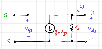
Most of the time, we are interested in the small signal behavior of our amplifiers, i.e. what happens to the amplifier voltages and currents as we introduce small disturbances (information carrying signals) at the input. To gain intuition and to facilitate circuit analysis using nonlinear devices, we linearize our circuits to obtain the two-port model shown in Fig. 1. For MOSFETs at low frequencies, the two-port model is composed of the transconductance, and the output resistance.
Transconductance
Transconductance is defined as:
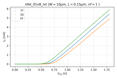
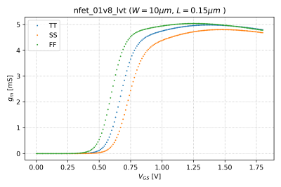
This is the slope of the transfer characteristic curves. Thus, by numerically differentiating the vs. curve shown in Fig. 2 for an NMOS transistor with a width , a length , and with , we can obtain the transconductance plot shown in Fig. 3.
Output Resistance
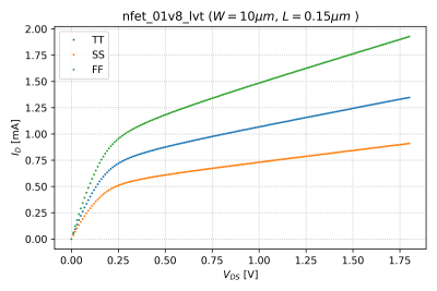
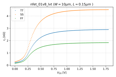
Similarly, we can take the derivative of the output characteristics, shown in Fig. 4 for , to get the output resistance, which is defined as:
The output resistance as a function of is shown in Fig. 5 for .
Answer the following questions:
- Given the transconductance plot in Fig. 3, why is there a peak in the transconductance curve? What is causing this?
- Generate Fig. 3, but on a logarithmic y-axis. Is this what you expect for ? Explain.
- Plot for and . Does the transconductance change with ? Is this the behavior you expect? Explain.
- Plot the output resistance for and . Do you see any changes in the the effects of process variations? What do you think is causing this behavior?
Activity 2: Power Efficiency
Activity 3: PMOS Small Signal Parameters
Repeat Activity 1 for a 1.8V LVT PMOS transistor with the same dimensions as the NMOS transistor: a width , a length , and with .
